Fujitsu Laboratories Ltd. today announced the development of a new thin-film process technology that increases oxygen-producing efficiency by more than 100-fold. This is compared to using photocatalyst material, as is, with photoreactive electrodes that produce electricity and oxygen through the interaction of sunlight and water, used in artificial photosynthesis .
The results of this development could be used to increase energy storage capacity through artificial photosynthesis, and hold the promise of becoming a fundamental technology relating to energy and the environment, thus contributing to a more sustainable future with solutions to the problems of global warming and natural resource depletion.
Background
Reducing CO2 and other greenhouse gases and developing renewable energy that can be stored are urgent issues for building a society that will be sustainable in the future. Artificial photosynthesis uses sunlight, water, and CO2 to produce oxygen, hydrogen, and organic compounds that can be used as stored energy, making it the subject of increasing interest.
Issues
To artificially produce storable energy in the form of hydrogen and organic compounds requires efficiently extracting reaction electrons from a photocatalyst material using the energy in sunlight, and at the electrode, efficiently reacting with water or CO2. In the past, semiconductor materials and relatively coarse-grained photocatalyst materials have been used in low-density rigid structures for the photoreactive electrodes where sunlight and water react. However, as the usable wavelengths of light in sunlight (visible light) fall in a narrow range, it has been difficult to achieve a sufficient current flow from the chemical reaction.
About the Technology
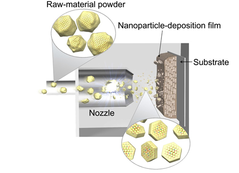
Fujitsu Laboratories has improved on methods for forming thin films (nanoparticle deposition(2)) of electroceramics on flexible mounting sheets to create capacitors and other passive elements. It has also developed a process technology for layering thin films on a substrate using a nozzle to spray the raw-material photocatalyst-material particle that fragments the particle on a thin plate. Key features of the technology are as follows. Analyses of the internal structure of the material were performed jointly with the Crystal Interface Laboratory at the University of Tokyo.
1. Expands the usable wavelengths of sunlight
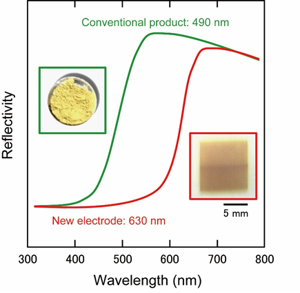
After creating a film of the raw-material photocatalyst-material particle, it is formed into a crystalline structure having deviation at the molecular level, which broadens the spectrum of sunlight that can be absorbed from a maximum wavelength of 490nm using existing technology to 630nm with this technology, more than doubling the usable sunlight that is captured (Figure 1).

Figure 1: Reflectivity of sunlight with the new material
2. High electrical conductivity
The film has a good crystalline structure lacking in macro- or micro-level flaws, and a precisely formed structure with excellent electrical conductivity between the particles in the material (Figure 2). This enables electrons electrically excited by photons in sunlight to be efficiently transmitted to the electrodes.

Figure 2: Process technology for film with high electrical conductivity
3. A structure formed of nano-sized particles ensures a large surface area to react with water
The film’s surface structure increases the surface area that can react with water, and is formed into a systematically structured crystalline surface that boosts electron density throughout the material’s crystal structure. This effectively promotes much greater interaction between water and sunlight (Figure 3).
![Figure 3: Structure of light-reacting electrodes for artificial photosynthesis [High electron density crystal layer is highly structured and near film surface] (Image courtesy Crystal Interface Laboratory at the University of Tokyo)](http://www.haptic.ro/wp-content/uploads/2016/12/nanoparticle.jpg)
Figure 3: Structure of light-reacting electrodes for artificial photosynthesis
[High electron density crystal layer is highly structured and near film surface] (Image courtesy Crystal Interface Laboratory at the University of Tokyo)
Results
Compared to using photocatalyst material as-is, this technology more than doubles the usable amount of light that can be gathered from sunlight, and increases by more than a factor of 50 the surface area of the material that can react with water. Taken together, these advances have been confirmed to increase the efficiency in producing electricity and oxygen by more than a factor of 100.
Future Plans
Fujitsu Laboratories is continuing to work on further advances in photocatalyst materials and process technology to improve the characteristics of photoreactive electrodes, and is working on developing technologies for the dark-reaction part (CO2-reducing reactions) and the overall system, with the goal of implementing artificial photosynthesis technology.
Fujitsu Laboratories seeks to contribute to a more sustainable society through renewable energies, and to develop the foundation for sustainable energies and the environment.
About Fujitsu
Fujitsu is the leading Japanese information and communication technology (ICT) company, offering a full range of technology products, solutions, and services. Approximately 156,000 Fujitsu people support customers in more than 100 countries. We use our experience and the power of ICT to shape the future of society with our customers. Fujitsu Limited (TSE: 6702) reported consolidated revenues of 4.7 trillion yen (US$41 billion) for the fiscal year ended March 31, 2016. For more information, please see http://www.fujitsu.com.
About Fujitsu Laboratories
Founded in 1968 as a wholly owned subsidiary of Fujitsu Limited, Fujitsu Laboratories Ltd. is one of the premier research centers in the world. With a global network of laboratories in Japan, China, the United States and Europe, the organization conducts a wide range of basic and applied research in the areas of Next-generation Services, Computer Servers, Networks, Electronic Devices and Advanced Materials. For more information, please see: http://www.fujitsu.com/jp/group/labs/en/.
Source: Fujitsu