An international collaboration of German, Israeli, and British teams has investigated the deposition of thin chalcopyrite layers. They were able to observe specific defects as these formed during deposition and under what conditions they self-healed using the BESSY II X-ray source at the Helmholtz Zentrum Berlin. The results of their research provide clues to optimising fabrication processes and have now been published in Energy & Environmental Science.
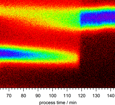
The data (photon energies over time) show defects (lower signal) which disappear after 120 minutes. This happens at the transition from the copper-poor phase to the copper-rich one. Credit: HZB
Copper-indium-gallium-selenide (CIGSe) solar cells have the highest efficiency of polycrystalline thin-film solar cells. The four elements comprising CIGSe are vapour-deposited onto a substrate together to form a very thin layer of tiny chalcopyrite crystals. It is an exceedingly complex process controlled by many variables. This is why CIGSe modules in standard industrial formats have not yet attained the record efficiency already demonstrated at laboratory scale. One possible cause: defects that reduce the efficiency level can form during the course of fabrication. A collaboration of German, Israeli, and British teams has now conducted detailed studies of how different fabrication techniques influence the microstructure. They were able for the first time to observe the defects as these formed during deposition and under what conditions they self-healed by using in-situ X-ray diffraction and fluorescence analysis capabilities at the BESSY II X-ray source.
Additional copper helps defects heal
Vapour deposition of thin CIGSe films is a complex process. Indium, gallium, and selenium are first deposited on the substrate. The deposition of the copper and selenium atoms takes place in a second step. These atoms migrate into the In-Ga-Se layer. Tiny CIGSe crystals of chalcopyrite form there. The concentration of copper only reaches the correct value over the course of this second step. The prior copper-poor phase is characterised by numerous defects within the crystal. The defects increasingly disappear with the addition of copper and selenium. If more copper and selenium atoms are added after reaching the “right” ratio, then these two elements no longer fit into the existing crystal matrix and deposit themselves as copper and selenium grains in and on the polycrystalline CIGSe layer. This is actually problematic, since the grains must be removed afterwards. Nevertheless, they apparently have an important function in reducing the defects to near zero, as the current work shows.
Analysing growing structures of elements in real time
Dr. Roland Mainz and his colleagues at HZB were able to observe the changes to the film structure during deposition using X-ray diffraction at the EDDI beamline of BESSY II – in real time. At the same time, they were able to use X-ray fluorescence to analyse the elemental composition of the thin-film layer as it grew. Simultaneous observation with two methods enabled them to obtain a new insight: “The annihilation of the defects takes place very rapidly – just prior to the excess copper-selenium grains being deposited on the surface of the CIGSe film and the film entering the copper-rich phase. So far, we had only understood the copper-rich phase as being important for the growth of the grains. Now we know that it also plays an important role in the elimination of the defects”, explains Mainz.
Improving vapour deposition processes for high-quality CIGSe films
Helena Stange, co-author of the study, simulated the influence of the various types of defects on the diffraction signal. The in-situ observations fit extremely well with the simulations and with the results derived from different imaging processes used to study the samples in various stages of deposition by teams at the Max Planck Institute for Solid State Research in Stuttgart, the SuperSTEM Lab in Daresbury, England, and at the Racah Institute, Jerusalem.
An additional important result is that the temperature during deposition represents a relatively uncritical parameter for defect elimination. As soon as the layer reaches the copper-rich state, it makes little difference whether the process takes place at 400 degrees Celsius or 530 degrees Celsius. This insight is also of assistance in improving the procedure for depositing onto large surface areas. Instead of trying to maintain as homogenous a temperature as possible over the entire surface, other parameters could be optimised.
The results have been published in Energy & Environmental Science Energy & Environmental Science publiziert: “Annihilation of structural defects in chalcogenide absorber films for high-efficiency solar cells” DOI: 10.1039/C6EE00402D
The collaboration is part of the Helmholtz Virtual Institute of “Microstructure control for thin-film solar cells” that has been funded from 2012 to 2018.
Source: Helmholtz Zentrum Berlin